The global electric vehicle Onboard Charger (OBC) market is estimated to reach $10.82 billion by 2027, registering a CAGR of 22.4% from 2020 to 2027. With OBCs that on average give 25% higher DC-DC rating and ~30% reduction in charge duration, Electra EV has been developing OBCs which have helped electric mobility applications exceed end-user expectations.
Role of Onboard Charger
The main function of an onboard charger, is to manage the flow of current from the grid to the traction battery. On board chargers (OBCs) helps in charging the electric vehicles from any source. Hence, electric vehicles do not have to depend on charging stations all the time.
Another function of OBC is that it controls the level of current and voltage at which the battery is charged. There are mainly two types of charging : constant voltage and constant current charging. Even though constant current charging provides high efficiency and high charging speed it can affect the lifespan of the battery. This is due to over-charging. In the case of constant voltage charging, there is a chance that a high amount of current can flow into the battery initially.
The above problem can be solved by charging the battery initially by constant current charging. Then after reaching a certain amplitude, the battery is charged using constant voltage charging. This charging strategy is the most important role of an EV on board charger.
Onboard Charger in Different Charging Stations
Role of OBC in AC Charging
In AC charging level 1 and level 2, the AC power from the grid is converted to DC power by the OBC to charge the battery via the Battery Management System(BMS). The voltage and current regulation is performed by the OBC. In addition, the disadvantage of AC charging is as its charging time increases, the power output becomes low.
The charging rate, or required input current, is determined by the EV itself in AC chargers. Because not all electric vehicles (EVs) require the same amount of input charging current, the AC Charger must communicate with the EV to determine the required input current and establish a handshake before charging can commence. This communication is referred to as Pilot wire communication. The Pilot wire identifies the type of charger attached to the EV and sets the OBC’s required input current.
Role of OBC in DC Charging
In DC fast charging or Level 3 charging, the AC power from the grid is directly supplied to the Battery Pack. As shown in the figure above, we can see that there is a AC/DC converter in-built in the DC charger itself. Hence it eliminates the need for OBC in this level of charging. Therefore, this helps in reducing the charging time. The EVSE is arranged in stacks to deliver high current because a single stack will not be able to supply high current. Hence, there is no role of OBC in DC Charging.
Types of On Board Charger
There are mainly two types of EV on board chargers :
●Single phase On board Charger
●Three phase EV Onboard Charger
This classification is based on the number of phases it can use. The output of a standard single phase OBC is 7.2-7.4 kWh. While, that of a three-phase OBC is 22kWh. As a matter of fact, the OBC is able to detect which type of input it can accept. When connected to only one phase, the power that this on board charger can tolerate is 110 – 260 V AC (and 360 – 440V in the case of using three phases). The battery receives a voltage between 450 and 850 volts as an output.
Working of an Onboard Charger
In OBCs using a rectifier, high power AC input is converted to DC power and provides Power Factor Correction. To boost the power factor to unity, a power factor correction (PFC) circuit removes harmonic distortion in the supply current and provides a current waveform that is close to a basic sine wave. This section of the charger determines whether it can use one, two, or all three alternating current phases. In addition, the DC/DC converter must isolate the power grid from the HV dc bus and the HV dc bus from the LV dc bus for safety reasons.
The second phase receives the 700V output voltage. The resultant DC signal is chopped into a square wave, that drives a transformer. This further provides the required DC voltage. An isolated CAN bus can be used to monitor and control the entire system. Digital isolators and digital isolators with integrated DC/DC power converters are used to isolate the CAN. Finally, the required voltage is supplied to the battery.
Design Considerations of OBCs
●To maximise range, inverters need to be extremely efficient yet at the same time be as small as possible, often with multiple dies per switch (4 – 8) and multiple switches per inverter cell
●Using GaN FETs eliminates the need for a separate body diode in the inverter switches.
●AC outlet - usually fixed frequency and voltage amplitude, passive filter required for high signal fidelity and low distortion (low THD)
GaN FETs
Whether for low- or high-power conversion applications, Power Gallium Nitride FETs (GaN FETs) are increasingly making their way into mainstream markets. For a variety of 650 V and 150 V applications GaN FETs deliver the fastest transition / switching capability (highest dv/dt and di/dt), and best power efficiency. Additionally, Nexperia power GaN FETs bring enhanced power density through reduced conduction and switching losses.
Targeted at high-voltage / high-power applications, Nexperia cascode GaN FETs provide exceptionally high switching frequency capability for 650 V applications and the robust low on-resistance particularly suited for automotive electrification. For 650 V and ≤ 150 V industrial and consumer applications, Nexperia e-mode GaN FETs provide the balance between switching performance and robustness.
Low voltage e-mode GaN FETs
Delivering optimum flexibility in power systems, Nexperia e-mode GaN FETs are ideal for high-power <200 V applications. Offering superior switching performance due very low QC and QOSS values. Enabling faster charging for e-mobility and wired / wireless changing systems as well as significant space and BOM savings in LiDAR and lower noise in Class D audio amplifiers.
Produts
GAN3R2-100CBE:The GAN3R2-100CBE is a a general purpose 100 V, 3.2 mΩ Gallium Nitride (GaN) FET in a 15 bump Wafer Level Chip-Scale Package (WLCSP). It is a normally-off e-mode device offering superior performance.
GAN7R0-150LBE:The GAN7R0-150LBE is a general purpose 150 V, 7 mΩ Gallium Nitride (GaN) FET in a Land Grid Array (LGA) package. It is a normally-off e-mode device offering superior performance.
650 V e-mode GaN FETs
Delivering optimum flexibility in power systems, Nexperia e-mode GaN FETs are ideal for low-power 650 V applications. Offering superior switching performance due very low QC and QOSS values, they bring improved efficiency to 650 V AC/DC and DC/AC power conversion. As well as bringing significant space and BOM savings in BLDC and micro servo motor drives or LED drivers.
Produts
GAN080-650EBE:The GAN080-650EBE is a general purpose 650 V, 80 mΩ Gallium Nitride (GaN) FET in a DFN 8 mm x 8 mm surface mount package. It is a normally-off e-mode device offering superior performance.
GAN140-650EBE:The GAN140-650EBE is a general purpose 650 V, 140 mΩ Gallium Nitride (GaN) FET in a DFN 8 mm x 8 mm surface mount package. It is a normally-off e-mode device offering superior performance.
GAN140-650FBE:The GAN140-650FBE is a general purpose 650 V, 140 mΩ Gallium Nitride (GaN) FET in a DFN 5 mm x 6 mm surface mount package. It is a normally-off e-mode device offering superior performance.
650 V cascode GaN FETs
The very high electron mobility of GaN enables the creation of devices with low on-resistance and exceptionally high switching frequency capability. These advantages are vital in next-generation power systems, such as industry 4.0 and renewable energy applications. Nexperia cascode GaN FETs are the enabler in these applications offering high power density, high performance, and high switching frequency. This unique solution facilitates the ease of driving the devices using well-known Si MOSFET gate drivers. Additionally, they deliver unmatched high junction temperature (Tj [max] 175 °C), ease of design freedom and improved reliability of power systems.
Produts
GAN039-650NBB:The GAN039-650NBB is a 650 V, 33 mΩ Gallium Nitride (GaN) FET in a CCPAK1212 package. It is a normally-off device that combines Nexperia’s latest high-voltage GaN HEMT H2 technology and low-voltage silicon MOSFET technologies — offering superior reliability and performance.
GAN039-650NTB:The GAN039-650NTB is a 650 V, 33 mΩ Gallium Nitride (GaN) FET in a CCPAK1212i inverted package. It is a normally-off device that combines Nexperia’s latest high-voltage GaN HEMT H2 technology and low-voltage silicon MOSFET technologies — offering superior reliability and performance.
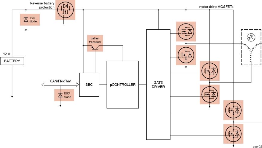
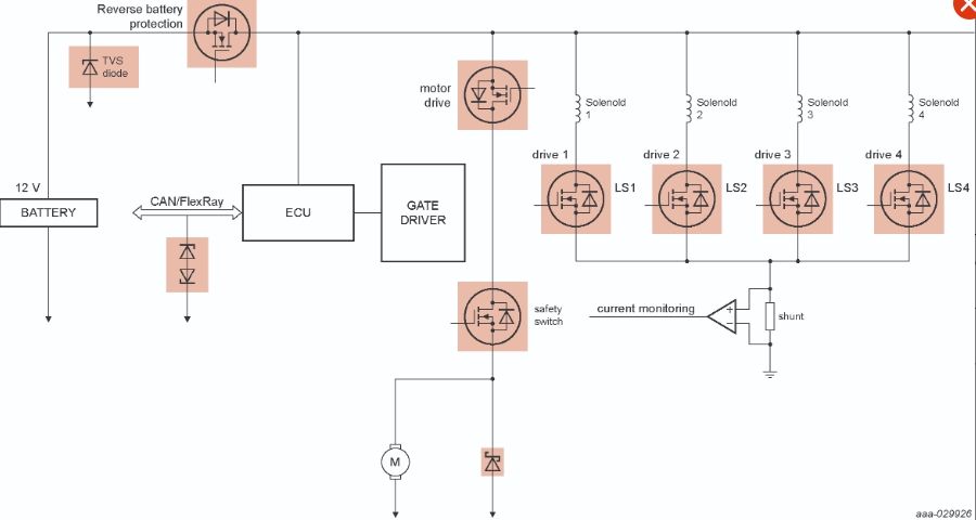
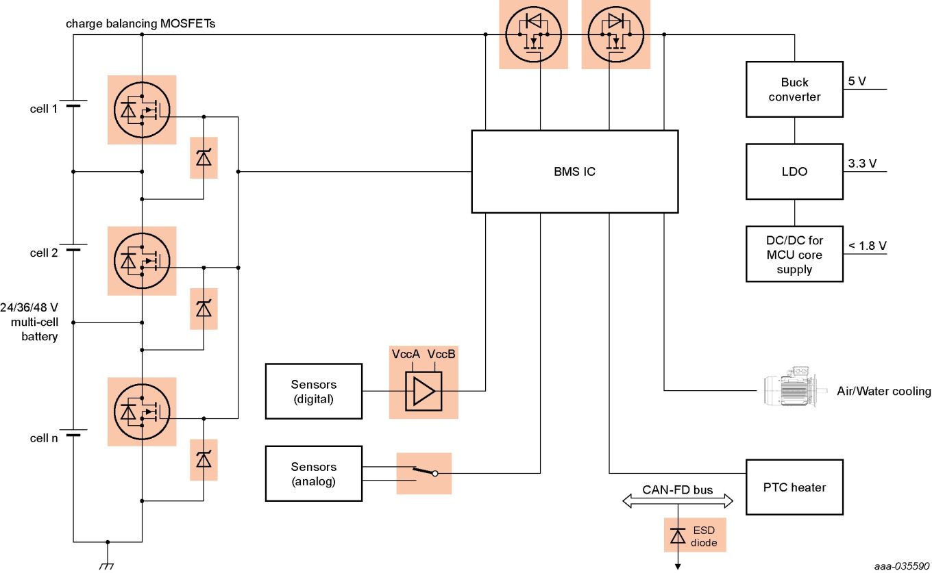
LIN/CAN(FD)/FlexRay
In-vehicle networks consists of multiple mircoprocessors communicating over different networks. LIN/CAN(FD)/FlexRay are highly reliable in-vehicle network protocols to handle the car's physically challenging environment. Nexperia offers dedicated ESD protection devices meeting emission, immunity and signal integrity requirements to ensure safe operation.
Growth of OBC in the automotive industry
During the period 2020-2025, the worldwide automotive EV onboard charger market is expected to grow at a CAGR of around 30%.In the projected term, growing sales of electric vehicles, strict pollution laws, developments in battery technology, and improved charging infrastructure are expected to boost demand for automotive onboard chargers. Electric passenger vehicles are already being adopted in developed nations, and new startups and significant players in the EV sector are aiming to launch their own new electric models in the next years.
Studies and developments are focusing on developing more efficient and light weight onboard chargers. Because development can help in the advancement of electric vehicle industry. Many established and emerging countries have framed their green mobility plans, which include prohibiting diesel vehicles and providing incentives to buyers of electric vehicles. By 2030, India intends to prohibit all diesel-powered vehicles off the roadways.
Previous: Electric power steering (EPS)
Next: ADAS Radar Sensor: How it Works & Why it Needs Calibration